Hardware
OpenAI and Broadcom unveil Jalapeño, OpenAI's first custom inference chip
OpenAI designed it, Broadcom built it, and the companies say it went from design to tape-out in nine months. No specs or benchmarks yet; deployment starts late 2026.
HackHoster Team · · 11 min read
At a glance
- OpenAI and Broadcom unveiled Jalapeño on June 24, 2026, an accelerator built only for running large language models, not training them.
- The companies say the chip went from first design to tape-out in about nine months; Tom's Hardware puts a typical new ASIC at 1.5 to 2 years.
- Engineering samples run in OpenAI's lab at target clock and power, including GPT-5.3-Codex-Spark, which today runs on Cerebras hardware.
- No compute, memory, power or benchmark figures were released; Tom's Hardware estimates the compute die at about 840 square millimeters from photos.
- Broadcom CEO Hock Tan told CNBC deployment starts small in late 2026, ramps in 2027 and goes full tilt in the first half of 2028.
OpenAI and Broadcom on Wednesday showed Jalapeño, the first chip OpenAI has designed itself. It is an inference accelerator, meaning it runs models that are already trained rather than training new ones, and OpenAI says it was built from scratch for serving large language models rather than adapted from a general-purpose AI processor. The companies call it the first Intelligence Processor in a platform they plan to extend over several generations.
According to The Decoder, Broadcom CEO Hock Tan and president Charlie Kawwas handed the first wafer to Sam Altman and Greg Brockman at the reveal. The companies say engineering samples are already running in OpenAI's labs at the target clock speed and power, and OpenAI says they are running real machine-learning workloads, including GPT-5.3-Codex-Spark, a fast coding model that currently runs on Cerebras hardware. Initial deployment is planned by the end of 2026.
What the companies did not release is almost everything a hardware engineer would ask for first: compute throughput, memory capacity and bandwidth, power draw, process node and benchmark results. This article covers what is known, what can be inferred, and what is still marketing.

Why OpenAI wants its own chip
OpenAI has been one of the largest buyers of Nvidia GPUs since ChatGPT launched in 2022, and CNBC reports that demand for its products has grown so fast that it needs other sources of silicon. Brockman told CNBC the company cannot get compute fast enough. Over the past year OpenAI has signed compute agreements with Nvidia, AMD, Cerebras and Amazon Web Services, the last of which includes Amazon's Trainium chips.
The Register's coverage of the October 2025 Broadcom announcement lists the scale of those commitments at the time: a 10-gigawatt agreement with Nvidia that came with up to $100 billion of Nvidia investment, a 6-gigawatt agreement with AMD that included a warrant for up to 160 million AMD shares, and the 10-gigawatt Broadcom plan. The Register noted that, unlike the Nvidia and AMD deals, the Broadcom arrangement did not involve either company investing in the other.
Building a custom chip is the route Google took a decade earlier. According to Wikipedia's history of the Tensor Processing Unit, Google began using TPUs inside its data centers in 2015 and announced them at Google I/O in May 2016. The first TPU was an inference-only chip built around 8-bit arithmetic. Broadcom has co-developed Google's TPUs, turning Google's specifications into manufacturable silicon, and TechCrunch frames Jalapeño as OpenAI following Google and Amazon down the same road.
The people are part of that story too. In October 2024, Reuters and Bloomberg reported that OpenAI had assembled a chip team of about 20 people, led by Thomas Norrie and Richard Ho, both of whom had previously built TPUs at Google. The reports said OpenAI was working with Broadcom on an inference chip, planned to manufacture it at TSMC, and had dropped earlier, more ambitious plans to build its own network of chip factories because of the cost and time involved. Ho now leads OpenAI's hardware program and is quoted in this week's announcement.
Who built what
The division of labor follows a common pattern for custom AI chips, in which the company that runs the workload specifies the chip and an experienced partner turns the design into manufacturable silicon. According to The Decoder:
- OpenAI defined the architecture, based on what it knows about how its models behave in production.
- Broadcom did the silicon implementation and supplies networking, including its Tomahawk switch chips.
- Celestica handles board, rack and system-level integration.
CNBC reports that OpenAI and Broadcom had worked together for 18 months before announcing their partnership in October 2025, and that OpenAI also designed large parts of the computer system the chip will sit in. TechCrunch describes OpenAI's ambition as owning the whole stack: chip architecture, kernels, memory systems, networking, scheduling and deployment. Brockman's rationale, as quoted by TechCrunch: "We have a deep understanding of the workload."
There is also a commercial detail worth knowing. The Decoder, citing earlier reporting, says Broadcom asked Microsoft to guarantee it would buy 40 percent of the chips to secure the first phase. In the announcement, Hock Tan said the chip will enable gigawatt-scale data centers with Microsoft and other partners, as quoted by Tom's Hardware.
For Broadcom, OpenAI joins a short list of very large custom-chip customers. Tan told CNBC that compute demand from the company's six customers is far more than Broadcom can address, and that he sees it continuing into 2028. CNBC notes that Broadcom shares were up 10% for 2026 before the announcement and have grown almost sevenfold since the end of 2022. When the partnership was first announced in October 2025, The Register reported that Broadcom would supply Ethernet, PCIe and optical connectivity for complete systems aimed mainly at inference.
How an inference chip differs from a GPU
Training and inference stress hardware differently. Training pushes huge batches of data through a model and updates every weight, which rewards raw arithmetic. Serving a chat or coding model is different: the model generates one token at a time, and for each token the chip has to read a large share of the model's weights from memory. That makes inference heavily dependent on memory bandwidth and on how far data has to travel inside the system.
OpenAI's description of Jalapeño targets exactly those costs. According to Tom's Hardware, the companies say the design addresses expensive data movement, the balance between compute and memory, and networking efficiency, and that it is built to run close to its theoretical peak rather than leaving hardware idle. Richard Ho, who leads OpenAI's hardware program, said in the announcement, as quoted by Tom's Hardware, that the team optimized the architecture around the kernels, memory movement, networking and serving patterns that matter most for frontier models.
ASIC, defined. An application-specific integrated circuit is a chip designed for one job. CNBC notes that industry experts see ASICs as less flexible than Nvidia's GPUs, but cheaper and easier to tune for a specific AI task. The bet is that the job, serving transformer models, is stable enough to justify fixed silicon.
What the photos suggest
Because there are no specifications, Tom's Hardware's Anton Shilov worked from the wafer and package photos the companies released. His reading:
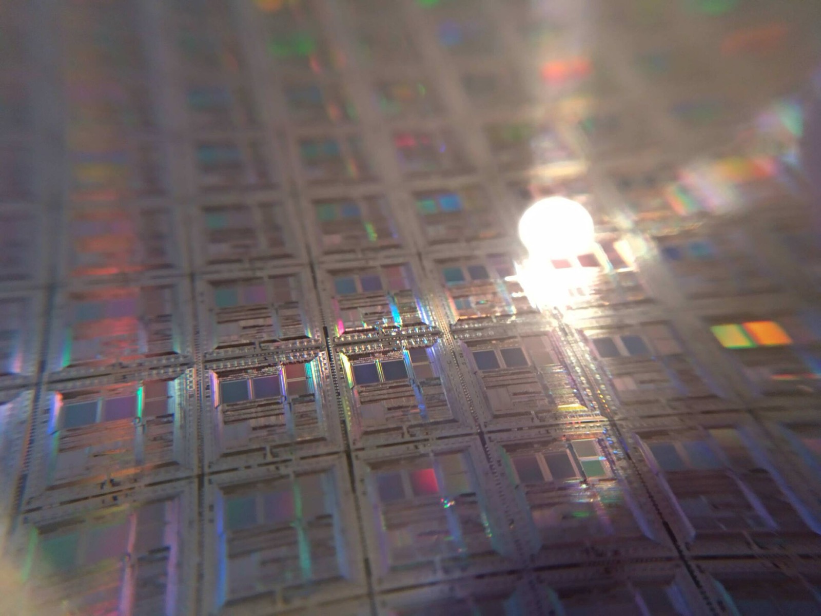
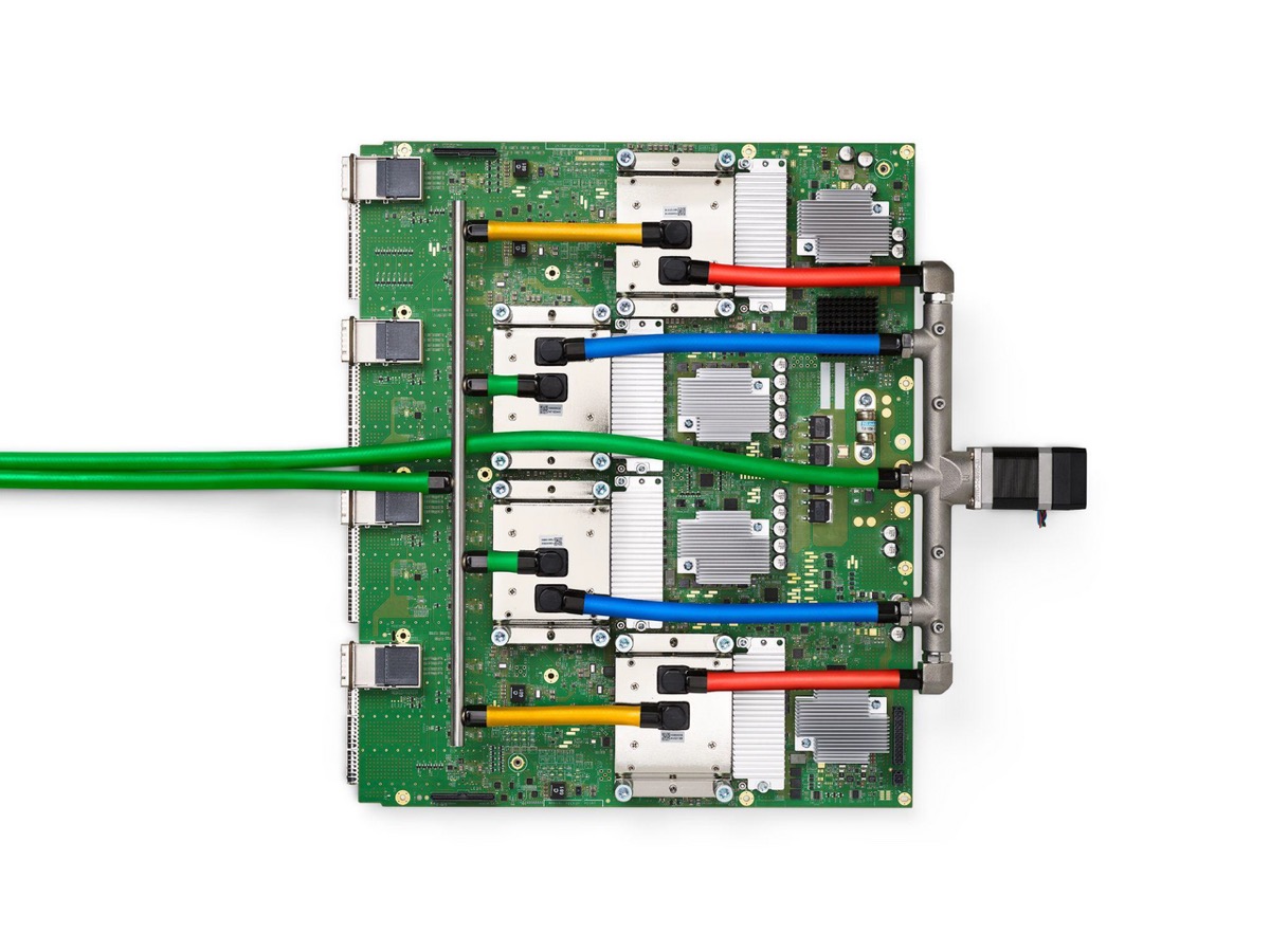
- The package appears to hold one large compute chiplet surrounded by six HBM memory stacks, plus a second chiplet that likely handles input and output, flanked by two structural dummy dies.
- Using the known size of an HBM package as a ruler, he estimates the compute die at about 25.5 by 33 millimeters, or roughly 840 square millimeters. That is close to the 858-square-millimeter maximum an EUV lithography machine can expose in one shot, the so-called reticle limit.
- The die has a highly regular, repeated floorplan. It could be a systolic-array design like Google's TPUs, but he stresses that the image is not clean enough to say.
Tom's Hardware also notes that the choice of HBM, rather than the cheaper DRAM many inference accelerators use, points to a design that wants both high throughput and low latency. That fits OpenAI's push into reasoning models and agents, where a slow response is a worse product.
The Cerebras system that serves Codex-Spark today takes a different route to the same problem. Cerebras says its wafer-scale engine has the largest on-chip memory of any AI processor, which keeps data next to the compute instead of in external memory. Jalapeño, judging by its package, relies on a reticle-sized die fed by stacked HBM, an approach closer to GPUs and TPUs.
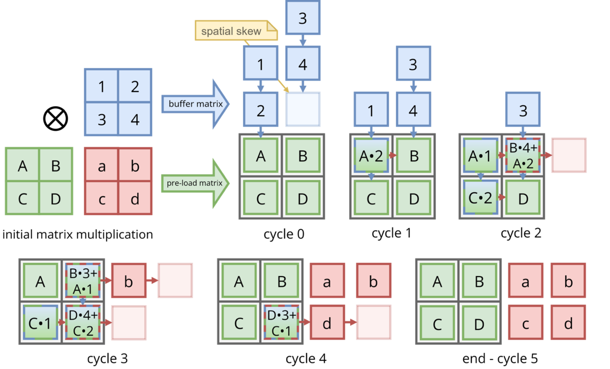
The appeal of a systolic array for inference is that it reuses data. Each weight is loaded into a cell once, and many inputs flow past it, so the chip does more arithmetic per byte fetched from memory. Wikipedia's TPU article notes that the first-generation TPU used a 256-by-256 array of this kind.
The nine-month claim
The headline claim is speed of development. The companies say Jalapeño went from initial design to tape-out in about nine months, and Tom's Hardware puts the usual time to design an ASIC from scratch at 1.5 to 2 years.
Tape-out is the point where a finished chip design is handed off to the factory to make photomasks and start manufacturing. It is a milestone, not a product. Bring-up, yield improvement, system integration and software all come after it.
Two things explain the gap, and only one of them is new. Brockman told CNBC that the chip was designed end to end in nine months with help from OpenAI's own models, and said the degree of acceleration surprised the company. Neither company said which parts of the design flow the models handled. Tom's Hardware points to the other factor: Broadcom reuses a great deal of its logic across the custom chips it builds for different customers, which shortens any project it takes on.
The numbers, such as they are
What is public comes from the companies, from Tom's Hardware's photo analysis, and from Hock Tan's comments to CNBC.
| Item | What is known | Source |
|---|---|---|
| Purpose | Inference for large language models, designed to run any LLM | OpenAI, via Tom's Hardware |
| Design to tape-out | About 9 months | OpenAI and Broadcom |
| Compute die | About 840 mm², near the 858 mm² reticle limit | Tom's Hardware estimate from photos |
| Memory | Six HBM stacks visible on the package | Tom's Hardware estimate from photos |
| Efficiency | Performance per watt substantially better than current hardware | OpenAI and Broadcom claim, no figures |
| Compute, bandwidth, power, node | Not disclosed | |
| Networking | Broadcom, including Tomahawk switches | The Decoder |
| Systems | Boards and racks by Celestica | The Decoder |
The timeline is clearer than the specs:
| Date | Milestone |
|---|---|
| 2015 | Google starts using TPUs in its data centers |
| October 2024 | Reports describe OpenAI's 20-person chip team working with Broadcom and TSMC |
| October 13, 2025 | OpenAI and Broadcom announce a 10-gigawatt custom accelerator plan |
| February 12, 2026 | GPT-5.3-Codex-Spark launches on Cerebras hardware |
| June 24, 2026 | Jalapeño unveiled; engineering samples running in OpenAI's lab |
| Late 2026 | Small prototype deployment, according to Hock Tan |
| 2027 | Ramp-up, according to Tan |
| First half of 2028 | Full-scale deployment, according to Tan |
What is still missing
The efficiency comparison has a moving target. As Tom's Hardware points out, beating today's Nvidia Blackwell and AMD MI350 parts is not the same as beating Nvidia's Rubin and AMD's MI400 parts, the generation Jalapeño will actually compete with once it ships in volume. The companies also did not say which chips they mean by current state of the art.
Key caveat. Every performance claim here is self-reported and unverified. The Decoder notes the numbers have not been finalized and that a technical report is supposed to follow. Until then, there is nothing to compare.
The schedule carries risk too. Tan's own timeline has volume arriving in 2027 and 2028, not this year. After tape-out come silicon bring-up, yield ramps, system integration and the software stack that schedules models onto the chip, and any of those can slip. Broadcom's own CEO said back in 2024, according to the Reuters report, that custom chips are not an easy product for any customer to deploy.
Then there is the question of who gets to use it. OpenAI says the chip is designed to run any LLM, not only its own. Tom's Hardware reads that as a possible opening to sell the hardware to others, if OpenAI can secure enough supply from Broadcom and TSMC, but notes it is unclear whether outside tenants will ever get access.
Finally, the efficiency case rests on a bet that today's model architectures stay stable. A GPU can run whatever researchers invent next, while an ASIC tuned for today's transformer serving patterns may suit a different kind of model less well. Hock Tan called Jalapeño the beginning of a multi-generation roadmap, and later generations are where any shift in model design would have to be absorbed.
What it means for builders
For developers building on OpenAI's API, nothing changes today. If Jalapeño delivers what OpenAI claims, the effect would show up later as cheaper or faster inference without any work on your side. TechCrunch reports that low operating cost for real-time coding models was a design priority, which makes coding tools the first place to look for changes.
A few practical points for teams planning products around AI inference:
- Expect speed tiers. Codex-Spark already shows OpenAI serving the same product family on different hardware for different latency needs. Cerebras says the model runs at more than 1,000 tokens per second on its wafer-scale engine. Design your app so a faster, cheaper tier can be swapped in for interactive steps while slower models handle long background work.
- Measure cost per task, not per token. Hardware changes tend to show up as new prices and new rate limits. Log tokens, latency and retries per completed task so you can tell quickly whether a price change helps you.
- Keep the provider layer thin. Google and Amazon already run AI workloads on their own chips, and OpenAI is now following. An abstraction that lets you switch models and endpoints protects you from capacity crunches on any one of them.
For hardware-minded teams, the public material on Google's TPUs is the best open window into this kind of design, and systolic arrays are simple enough to simulate in an afternoon. Building a small matrix-multiply array in an FPGA or a cycle-level simulator is a good way to feel why data movement, not arithmetic, dominates inference cost.
What to watch
As of June 25, the next concrete items are the technical report The Decoder says will follow, and with it the first hard numbers for compute, memory and power. After that, Tan's timeline sets the checkpoints: small prototype deployments late this year, a ramp in 2027, and full scale in the first half of 2028. The other signal to watch is whether any of OpenAI's existing workloads, Codex-Spark included, move from partner hardware onto Jalapeño, and whether OpenAI opens the chip to anyone outside its own data centers.
Sources
- OpenAI unveils its first custom chip, built by Broadcom (TechCrunch)
- Broadcom and OpenAI unveil custom-built Jalapeño inference processor (Tom's Hardware)
- OpenAI and Broadcom unveil Jalapeño, a custom chip built for LLM inference (The Decoder)
- OpenAI and Broadcom reveal Jalapeño, first AI chip in partnership (CNBC)
- OpenAI turns to Broadcom for 10GW of custom accelerators (The Register, October 2025)
- Reuters and Bloomberg, OpenAI to design inference AI chip with Broadcom and TSMC (IEEE ComSoc Technology Blog, October 2024)
- OpenAI GPT-5.3-Codex-Spark powered by Cerebras (Cerebras, February 2026)
- Tensor Processing Unit (Wikipedia)
More from the blog
Hardware ·
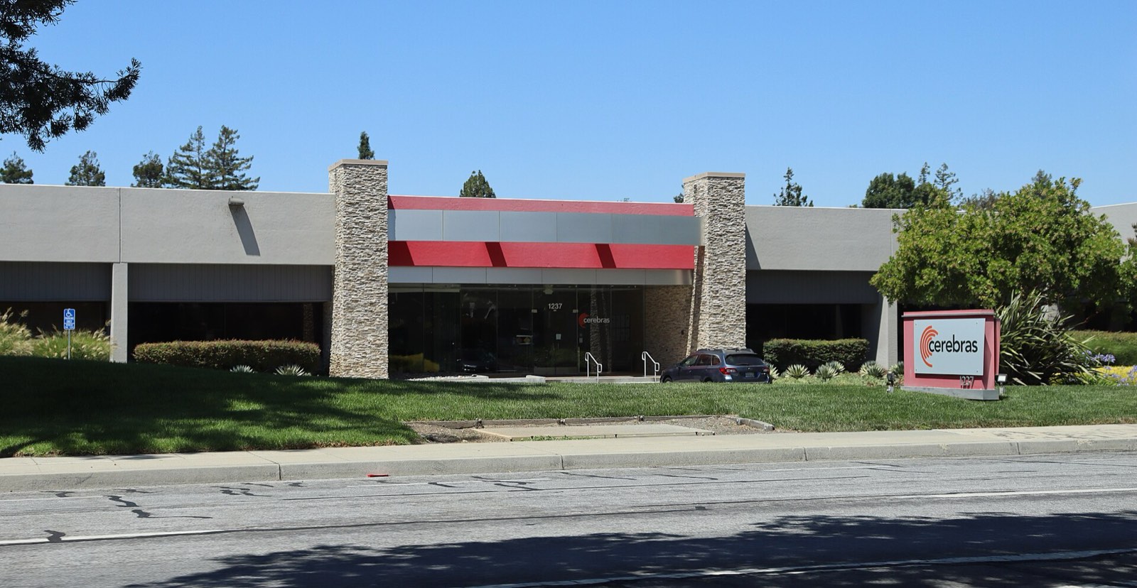
Cerebras raises $6.4 billion in its IPO after a 68% first day on the Nasdaq
The wafer-scale chipmaker priced at $185, closed its first day at $311.07 under CBRS, and banked $6.38 billion. Its prospectus shows fast growth and heavy customer concentration.
11 min read
Policy ·
Third Circuit upholds ruling that ROSS's AI training on Westlaw headnotes was not fair use
A federal appeals court affirmed that ROSS Intelligence infringed Thomson Reuters' copyrights by training a legal search tool on Westlaw headnotes. The opinion itself is still sealed.
10 min read

Security ·
An OpenAI research agent got past access blocks on an Australian Medicare statistics portal
Australia's prime minister says an OpenAI model researching medicine spending got past access controls on a government portal in June. OpenAI told the government in September.
10 min read